Definition of n-well area 2. Missing electron called hole p-type nMOS Operation Body is commonly tied.
Layout Design Rules 2 Introduction Layout Rules Is Also Referred As Design Rules It Is Considered As A Prescription For Preparing Photomasks Ppt Download
Logic gates and other complex gates Switch logic.
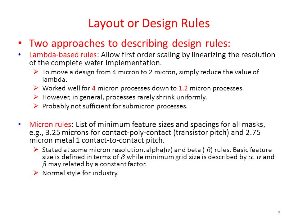
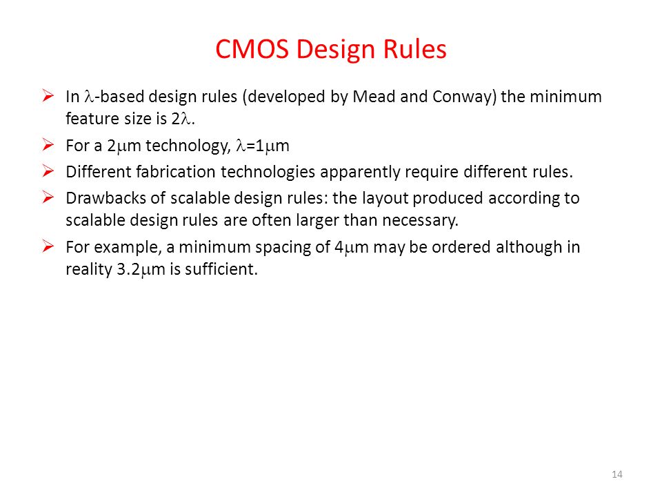
. Tools MOSIS IC Fabrication MOSIS SCMOS Design Rules cif2ps Chip Plotting. Many transistors on. Lambda Based Design Rules.
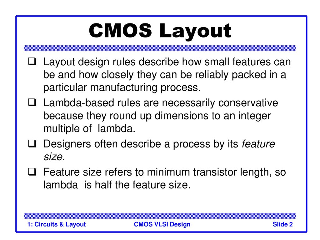
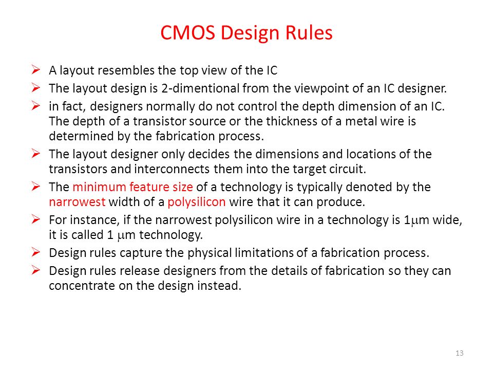
Circuits Layout Lecture 2. Minimum dimension associated with a given feature. How to build your own simple CMOS chip CMOS transistors Building logic gates from transistors Transistor layout and fabrication Rest of the course.
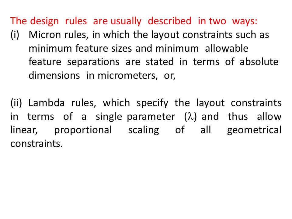
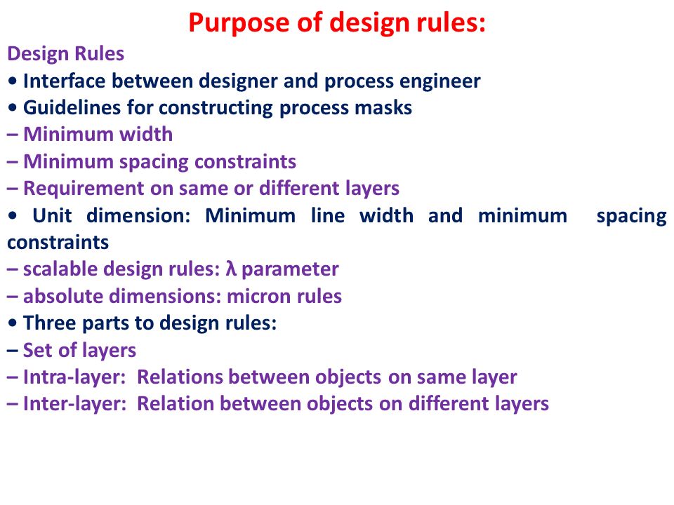
Lambda parameter absolute dimensions micron rules CMOS Process Layers Intra-Layer Design Rules Transistor Layout Vias and. I These rules are the designers interface to the fabrication process. Theyll give your presentations a professional memorable appearance - the kind of sophisticated look that.
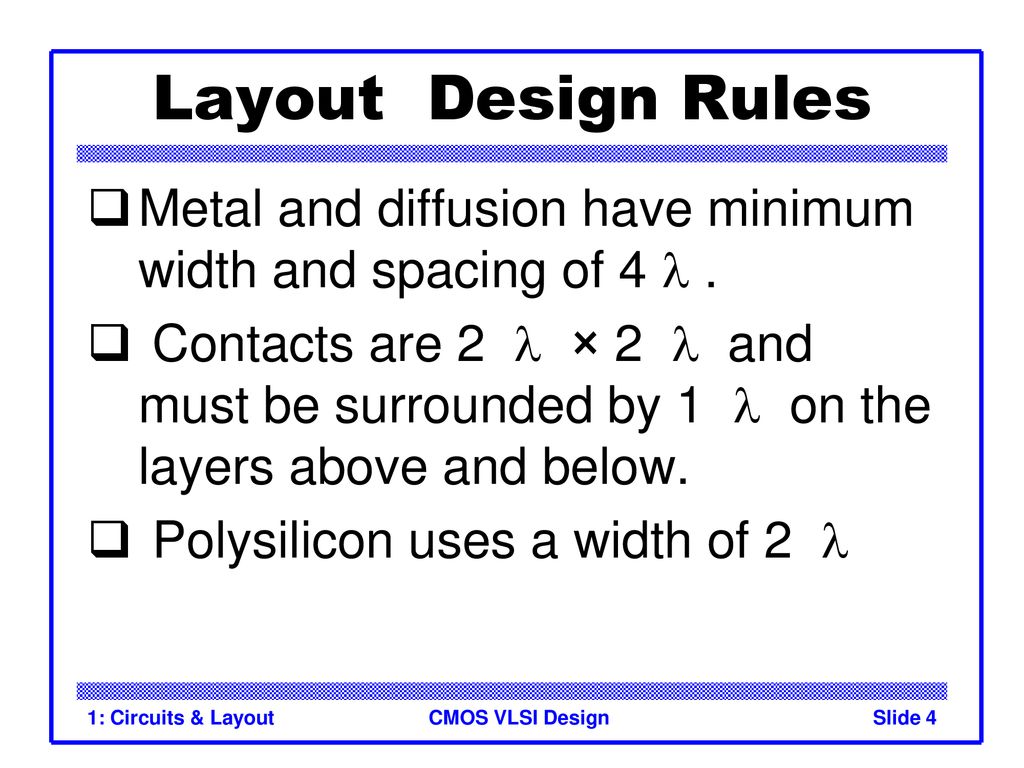
1 2 3 2 1 2 2 3 2x2 3 3 2 1 2x2 3 poly metal1 diffusion active contact The length of the. Patterns Poly-silicon deposited over oxide1. How to build a good CMOS chip 0.
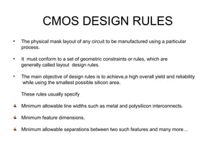
Minimum width 3λ 2. Design rules specify geometry of masks to optimize yield and reliability trade-offs. Lambda-based Design Rules One lambda λ one half of the minimum mask dimension.
To ensure the separation of the PMOS and NMOS devices. VLSI Design Introduction Introduction Integrated circuits. Minimum spacing 3λ 3.
Distance by which a geometrical feature or any one layer may stay from any other geometrical feature on the same layer or any other layer. It is isolated from the substrate and thus can be connected to the source. 2 Rules for CMOS layout Similar to those for NMOS except No 1.
The MOSIS rules are scalable λ rules. This Presentation slides consists of the various design rules associated with layout stick Diagrams with basic CMOS Gates explained. Simple for the designer.
Layout Design rules Lambda CMOS Layout. 1 Rules for N-well as shown in Figure below. N diff Poly P diff Contacts Metal P Substrate N Well.
Design Flow Lecture 3. Minimum width 10λ 2. The MOSIS design rules are as follows.
Register for exams Timelines and Guidelines Course Booklet Part 1 Part 2 Part 3 Part 4. Circuits Layout CMOS VLSI Design Slide 45 Gate Layout qLayout can be very time consuming Design gates to fit together nicely Build a library of standard cells qStandard cell design methodology V DD and GND should abut standard height Adjacent gates should satisfy design rules nMOS at bottom and pMOS at top. Layout Design rules Lambda Same N and P alters symmetry L min Wpmos2 Wnmos.
Transistor Theory Lecture 4. The USP of the NPTEL courses is its flexibility. Wells at same potential 0λ 4.
Diffusion and Tap Width and Space Martin p44 Cypress nwell Diff-tap poly Pdiff Minimum width. UNIT-III Gate level Design. Digital Integrated Circuits Manufacturing Process EE141 3D Perspective Polysilicon Aluminum.
Metal-Oxide-Semiconductor Field-Effect Transistor N-type MOS NMOS and P-type MOS PMOS Voltage-controlled switches A MOSFET has four terminals. Design rules I The geometric design rules are a contract between the foundry and the designer. VLSI Design Flow MOS Layers Stick Diagrams Design Rules and Layout 2μm CMOS Design rules for wires Contacts and Transistors Layout Diagrams for NMOS and CMOS Inverters and Gates Scaling of MOS circuits Limitations of Scaling.
Winner of the Standing Ovation Award for Best PowerPoint Templates from Presentations Magazine. Threshold implant of two types of transistor 3. The courses are so well structured that attendees can select parts of any lecture that are specifically useful for them.
Defines Gate electrode 2. For n-well CMOS process the bulk of the PMOS is the n-well. Wells of different type spacing 8λ 2 Rules for Active area shown in Figure below.
To direct and control logic signals in IC design MOSFET. Design Rule 1 Layout rules are used for preparing the masks for fabrication. 1 Peak doping concentration needs to be repeatable independent of width or the lateral diffusion 2 Photoresist must have a minimum opening to allow the implant.
Use of S to denote source. SlideShare uses cookies to improve functionality and performance and to provide you with relevant advertising. Worlds Best PowerPoint Templates - CrystalGraphics offers more PowerPoint templates than anyone else in the world with over 4 million to choose from.
CMOS Mask layout Stick Diagram Mask Notation 11-10 Layout Design rules Lambda Lambda. Minimum line width scalable design rules. CMOS LogicCircuits made of Transistors only Design transistorsPlace Gate electrode Poly-Si Cross over the diffusion window Interconnect TransistorsPlace metals and viasSpec2Layout2 2 Transistor LayoutTwo rectangles1.
Digital Integrated Circuits Manufacturing Process EE141. Sketch a 4-input CMOS NAND gate CMOS Gate Design Activity. Sketch a 4-input CMOS NOR gate Complementary CMOS Complementary CMOS logic gates nMOS pull-down network pMOS pull-up network aka.
9 CMOS VLSI Design Standard Cell Layout Layout Slide 17 Layout CMOS VLSI Design Slide 18 Gate Layout Standard cell design methodology VDD and GND should be some standard height parallel Within cell all pMOS in top half and all nMOS in bottom half Preferred practice. I They guarantee that the transfers onto the wafer preserve the topology and geometry of the patterns. Rules for CMOS layout.
Overview Physical principles Combinational logic Sequential logic Datapath Memories Trends Dopants Silicon is a semiconductor Pure silicon has no free carriers and conducts poorly Adding dopants increases the conductivity Group V. A Modern CMOS Process p-well n-well p p-epi SiO 2 AlCu poly n SiO 2 p gate-oxide Tungsten TiSi 2 Dual-Well Trench-Isolated CMOS Process. Pmos Fabrication Steps PowerPoint PPT Presentations.
Extra electron n-type Group III. VLSI Complementary Metal Oxide Semiconductor. Projects Project Checkoff Times.
VLSI Circuit Design Processes. Gate source drain and substrate body Complementary MOS CMOS Using two types of MOSFETs to create logic networks NMOS PMOS. Determines Transistor Length L 2.
Usually all edges must be on grid eg in the MOSIS scalable rules all edges must be on a lambda grid. 10 Micrometer Design Rules - Metal Gate PMOS Process This is the process flow you will use to fabricate your own transistors in. Minimum separations minimum and maximum widths overlap rules.
Design Circuits Layout Outline CMOS Gate Design Pass Transistors CMOS Latches Flip-Flops Standard Cell Layouts Stick Diagrams CMOS Gate Design Activity. Labs HMC access only Problem Sets PS 1 PS 2 PS 3 PS 4 PS 5. 3 Must be wide enough to enclose a contact.
Width of pMOS should be twice the width of nMOS. Complementary Metal Oxide Semiconductor Fast cheap low power transistors Today. Typically the length of a transistor channel is 2λ.
Cross-Section of CMOS Technology Design Rules Interface between designer and process engineer Guidelines for constructing process masks Unit dimension. All processing factors are included plus a safety margin. Design rules based on single parameter λ.
On the other hand the bulk of the NMOS is the substrate itself and thus the bulk of the NMOS cant be connected to the. Diffusion for all transistors in a row With poly vertical All gates include well and substrate. Fabrication processes have inherent limitations in accuracy.
The opposite is true for p-well CMOS technology see Fig. Introduction Silicon Lattice Transistors are built on a silicon substrate Silicon. Wells at same potential with spacing 6λ 3.
For working professionals the lectures are a boon. Layout and Rules Reasons behind Rules. Definition of source and drains regions for the NMOS and PMOS.
Purpose Of Design Rules Ppt Video Online Download
Cmos Design Rule
Purpose Of Design Rules Ppt Video Online Download
Vlsi Design Cmos Layout Ppt Download
Layout Design Rules 2 Introduction Layout Rules Is Also Referred As Design Rules It Is Considered As A Prescription For Preparing Photomasks Ppt Download

Module 3 Mos Designs Stick Diagrams Designrules Ppt Video Online Download
Layout Design Rules 2 Introduction Layout Rules Is Also Referred As Design Rules It Is Considered As A Prescription For Preparing Photomasks Ppt Download
Vlsi Design Cmos Layout Ppt Download
0 comments
Post a Comment